- Home
-
Categories
- Agriculture
- Apparel
-
Beauty & Personal Care
- Baby Care
- Bath Supplies
- Beauty Equipment
- Body Art
- Breast Care
- False Eyelashes & Tools
- Feminine Hygiene
- Fragrance & Deodorant
- Hair Care & Styling
- Hair Extensions & Wigs
- Makeup
- Makeup Tools
- Maternity Care
- Men's Grooming
- Nail Supplies
- Oral Hygiene
- Other Beauty & Personal Care Products
- Personal Hygiene Products
- Sanitary Paper
- Shaving & Hair Removal
- Skin Care
- Skin Care Tool
-
Business Services
- Advertising
- Agency Services
- Assurance Services
- Auction
- Brokerage, Intermediary Service
- Business Travel Services
- Certification, Inspection & Credit Management
- Computer & Information Technology Services
- Construction Services
- Consulting
- Corporate Register & Transfer
- Design Services
- Education & Training
- Internet Service
- Labour & Employment
- Law Services
- Leasing Services
- Logistics Services
- Other Business Services
- Passport & Visa
- Processing Services
- Project Cooperation
- Public Relations Services
- Repairs & Maintenance
- Research & Development Services
- Royalties & License Services
- Supply Chain Management
- Telecommunication Services
- Trade Show Services
- Translation Services
-
Chemicals
- Adhesives & Sealants
- Admixture&Additives
- Agrochemicals
- Basic Organic Chemicals
- Biological Chemical Products
- Catalysts & Chemical Auxiliary Agents
- Chemical Reagents
- Coating&Paint
- Custom Chemical Services
- Daily Chemicals
- Flavour & Fragrance
- Inorganic Chemicals
- Non-Explosive Demolition Agents
- Organic Intermediate
- Other Chemicals
- Painting & Coating
- Pigment & Dyestuff
- Polymer
- Surface Treatment Chemicals
-
Construction & Real Estate
- Balustrades & Handrails
- Bathroom & Kitchen
- Building Boards
- Building Glass
- Ceilings
- Corner Guards
- Countertops,Vanity Tops & Table Tops
- Curtain Walls & Accessories
- Decorative Films
- Door, Window & Accessories
- Earthwork Products
- Elevators & Escalators
- Fireplaces,Stoves
- Fireproofing Materials
- Floor Heating Systems & Parts
- Flooring & Accessories
- Formwork
- Heat Insulation Materials
- HVAC Systems & Parts
- Ladders & Scaffoldings
- Masonry Materials
- Metal Building Materials
- Mosaics
- Mouldings
- Multifunctional Materials
- Other Construction & Real Estate
- Plastic Building Materials
- Real Estate
- Soundproofing Materials
- Stairs & Stair Parts
- Stone
- Sunrooms & Glass Houses
- Tiles & Accessories
- Timber
- Wallpapers/Wall Coating
- Waterproofing Materials
-
Consumer Electronics
- Blockchain Miners
- Camera, Photo & Accessories
- Chargers,Batteries & Power Supplies
- Commonly Used Accessories & Parts
- Computer Hardware & Software
- Earphone & Headphone
- Electronic Cigarettes
- Electronic Publications
- Home Audio, Video & Accessories
- Mobile Phone & Accessories
- Mobile Phone Parts
- Other Consumer Electronics
- Portable Audio, Video & Accessories
- Presentation Equipment
- Smart Electronics
- Speakers & Accessories
- TV Receivers & Accessories
- Video Games & Accessories
- Electrical Equipment & Supplies
-
Electronic Components, Accessories & Telecommunications
- Acoustic Components
- Amplifiers and Comparators
- Capacitors
- Connectors and Accessories
- Crystals, Oscillators and Resonators
- Development Systems
- Diodes, Transistors and Thyristors
- Displays, Signage and Optoelectronics
- EL Products
- Electronic Accessories & Supplies
- Electronic Data Systems
- Electronic Signs
- Electronics Stocks
- Filters
- Inductors
- Integrated Circuits
- Microcontrollers, Standard and Specialty
- Optoelectronic Displays
- Optoelectronics
- Other Electronic Components
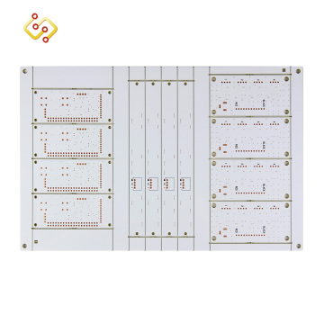
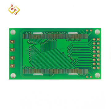
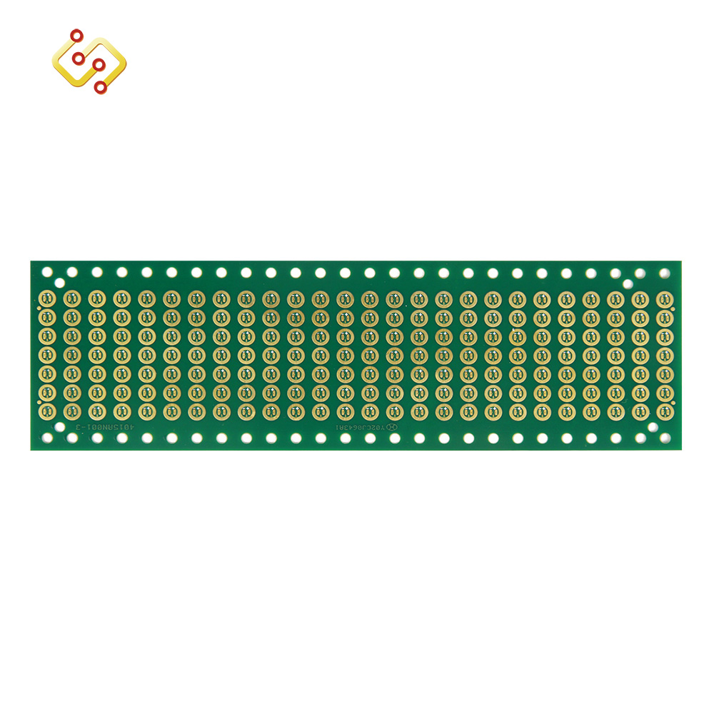
- PCB & PCBA
- Potentiometers
- Power Driver Modules
- Power Supplies and Circuit Protection
- Relay
- Resistors
- Sensors
- Switches
- Telecommunications
- Wireless & IoT
- Energy
- Environment
- Fabric & Textile Raw Material
- Fabrication Services
- Fashion Accessories
- Food & Beverage
- Furniture
- Gifts & Crafts
- Health & Medical
- Home & Garden
-
Home Appliances
- Air Conditioning Appliances
- Hand Dryers
- Home Appliance Parts
- Home Appliances Stocks
- Home Heaters
- Laundry Appliances
- Major Kitchen Appliances
- Other Home Appliances
- Personal Care & Beauty Appliances
- Refrigerators & Freezers
- Small Kitchen Appliances
- UV and Ultrasonic Cleaning Appliances
- Vacuum Cleaners & Floor Care
- Water Heaters
- Water Treatment Appliances
- Wet Towel Dispensers
- Home Textiles
- Lights & Lighting
-
Luggage, Bags & Cases
- Backpacks
- Bag & Luggage Making Materials
- Bag Parts & Accessories
- Briefcases
- Business Bags & Cases
- Evening Bags
- Handbags
- Handbags & Messenger Bags
- Luggage & Travel Bags
- Luggage Cart
- Messenger Bags
- Other Luggage, Bags & Cases
- Special Purpose Bags & Cases
- Sports & Leisure Bags
- Waist Bags
- Wallets & Holders
-
Machinery
- Agriculture Machinery & Equipment
- Air-Compressors & Parts
- Apparel & Textile Machinery
- Building Material Machinery
- Chemical & Pharmaceutical Machinery
- Cleaning Equipment
- Electric Equipment Making Machinery
- Electronic Products Machinery
- Electronics Production Machinery
- Energy & Mineral Equipment
- Engineering & Construction Machinery
- Environmental Machinery
- Food & Beverage Machinery
- Home Product Making Machinery
- Industrial Robots
- Industry Laser Equipment
- Machine Tool Equipment
- Machinery Accessories
- Machinery Service
- Material Handling Equipment
- Metal & Metallurgy Machinery
- Other Machinery & Industry Equipment
- Packaging Machine
- Paper Production Machinery
- Plastic & Rubber Processing Machinery
- Printing Machine
- Refrigeration & Heat Exchange Equipment
- Tobacco & Cigarette Machinery
- Welding Equipment
- Woodworking Machinery
-
Minerals & Metallurgy
- Aluminum
- Barbed Wire
- Billets
- Carbon
- Cemented Carbide
- Ceramic Fiber Products
- Ceramics
- Copper
- Fiber Products
- Fiberglass Products
- Glass
- Graphite Products
- Ingots
- Iron
- Lead
- Lime
- Magnetic Materials
- Metal Scrap
- Metal Slabs
- Mineral Wool
- Molybdenum
- Nickel
- Non-Metallic Mineral Deposit
- Ore
- Other Metals & Metal Products
- Other Non-Metallic Minerals & Products
- Pig Iron
- Quartz Products
- Rare Earth & Products
- Refractory
- Steel
- Titanium
- Tungsten
- Wire Mesh
- Zinc
-
Office & School Supplies
- Art Supplies
- Badge Holder & Accessories
- Board
- Board Eraser
- Book Cover
- Books
- Calculator
- Calendar
- Clipboard
- Correction Supplies
- Desk Organizer
- Drafting Supplies
- Easels
- Education Supplies
- Electronic Dictionary
- File Folder Accessories
- Filing Products
- Letter Pad / Paper
- Magazines
- Map
- Markers & Highlighters
- Notebooks & Writing Pads
- Office Adhesives & Tapes
- Office Binding Supplies
- Office Cutting Supplies
- Office Equipment
- Office Paper
- Other Office & School Supplies
- Paper Envelopes
- Pencil Cases & Bags
- Pencil Sharpeners
- Pencils
- Pens
- Printer Supplies
- Stamps
- Stationery Set
- Stencils
- Writing Accessories
- Yellow Page
-
Packaging & Printing
- Biodegradable Packaging
- Drug Packaging
- Gift Ribbon
- Glass Packaging
- Handles
- Logistics Packaging
- Metal Packaging
- Other Packaging Products
- Packaging Auxiliary Materials
- Packaging Design
- Packaging Rope
- Paper Packaging
- Plastic Packaging
- Printing Materials
- Printing Services
- Pulp
- Textile Packaging
- Wooden & Bamboo Packaging
- Rubber & Plastics
- Security & Protection
- Service Equipment
- Shoes & Accessories
-
Sports & Entertainment
- Amusement Park
- Artificial Grass & Sports Flooring
- Boats & Ships
- Cycling
- Fitness & Body Building
- Gambling
- Golf
- Indoor Sports
- Musical Instruments
- Other Sports & Entertainment Products
- Outdoor Sports
- Racquet Sports
- RVs & Campers
- Souvenirs
- Sports Bags
- Sports Safety
- Sports Shoes
- Team Sports
- Trade Show Tent
- Water Sports
- Winter Sports
- Timepieces, Jewelry, Eyewear
-
Tools & Hardware
- Abrasives
- Bearing Accessories
- Bearings
- Drill Bits
- Fasteners
- HVAC
- Hydraulic Tools
- Lab Supplies
- Machining
- Material Handling Tools
- Measuring & Gauging Tools
- Other Tool
- Pipe Fittings
- Pneumatic Tools
- Power Tool Accessory
- Power Tools
- Power Transmission Parts
- Pumps & Parts
- Test Instruments
- Testing Equipment
- Tool Parts
- Tool Sets
- Tool Storage
- Valve
- Welding & Soldering Supplies
- Hand Tools
- Hardware
-
Toys & Hobbies
- Action Figure
- Baby Toys
- Balloons
- Candy Toys
- Classic Toys
- Dolls
- Educational Toys
- Electronic Pets
- Fishing Toys
- Glass Marbles
- Light-Up Toys
- Noise Maker
- Other Toys & Hobbies
- Outdoor Toys & Structures
- Pretend Play & Preschool
- Solar Toys
- Toy Accessories
- Toy Animal
- Toy Guns
- Toy Parts
- Toy Robots
- Toy Vehicle
- Wind Up Toys
-
Vehicles & Accessories
- ATV/UTV Parts & Accessories
- Automotive Parts & Accessories
- Aviation Parts & Accessories
- Bus Parts & Accessories
- Container Parts & Accessories
- Go Kart & Kart Racer Parts & Accessories
- Heavy Duty Vehicle Parts & Accessories
- Marine Parts & Accessories
- Motorcycle Parts & Accessories
- New Energy Vehicle Parts & Accessories
- Railway Parts & Accessories
- Trailer Parts & Accessories
- Train Parts & Accessories
- Truck Parts & Accessories
- Universal Parts
- Vehicles & Transportation
- Home
-
Categories
- Agriculture
- Apparel
-
Beauty & Personal Care
- Baby Care
- Bath Supplies
- Beauty Equipment
- Body Art
- Breast Care
- False Eyelashes & Tools
- Feminine Hygiene
- Fragrance & Deodorant
- Hair Care & Styling
- Hair Extensions & Wigs
- Makeup
- Makeup Tools
- Maternity Care
- Men's Grooming
- Nail Supplies
- Oral Hygiene
- Other Beauty & Personal Care Products
- Personal Hygiene Products
- Sanitary Paper
- Shaving & Hair Removal
- Skin Care
- Skin Care Tool
-
Business Services
- Advertising
- Agency Services
- Assurance Services
- Auction
- Brokerage, Intermediary Service
- Business Travel Services
- Certification, Inspection & Credit Management
- Computer & Information Technology Services
- Construction Services
- Consulting
- Corporate Register & Transfer
- Design Services
- Education & Training
- Internet Service
- Labour & Employment
- Law Services
- Leasing Services
- Logistics Services
- Other Business Services
- Passport & Visa
- Processing Services
- Project Cooperation
- Public Relations Services
- Repairs & Maintenance
- Research & Development Services
- Royalties & License Services
- Supply Chain Management
- Telecommunication Services
- Trade Show Services
- Translation Services
-
Chemicals
- Adhesives & Sealants
- Admixture&Additives
- Agrochemicals
- Basic Organic Chemicals
- Biological Chemical Products
- Catalysts & Chemical Auxiliary Agents
- Chemical Reagents
- Coating&Paint
- Custom Chemical Services
- Daily Chemicals
- Flavour & Fragrance
- Inorganic Chemicals
- Non-Explosive Demolition Agents
- Organic Intermediate
- Other Chemicals
- Painting & Coating
- Pigment & Dyestuff
- Polymer
- Surface Treatment Chemicals
-
Construction & Real Estate
- Balustrades & Handrails
- Bathroom & Kitchen
- Building Boards
- Building Glass
- Ceilings
- Corner Guards
- Countertops,Vanity Tops & Table Tops
- Curtain Walls & Accessories
- Decorative Films
- Door, Window & Accessories
- Earthwork Products
- Elevators & Escalators
- Fireplaces,Stoves
- Fireproofing Materials
- Floor Heating Systems & Parts
- Flooring & Accessories
- Formwork
- Heat Insulation Materials
- HVAC Systems & Parts
- Ladders & Scaffoldings
- Masonry Materials
- Metal Building Materials
- Mosaics
- Mouldings
- Multifunctional Materials
- Other Construction & Real Estate
- Plastic Building Materials
- Real Estate
- Soundproofing Materials
- Stairs & Stair Parts
- Stone
- Sunrooms & Glass Houses
- Tiles & Accessories
- Timber
- Wallpapers/Wall Coating
- Waterproofing Materials
-
Consumer Electronics
- Blockchain Miners
- Camera, Photo & Accessories
- Chargers,Batteries & Power Supplies
- Commonly Used Accessories & Parts
- Computer Hardware & Software
- Earphone & Headphone
- Electronic Cigarettes
- Electronic Publications
- Home Audio, Video & Accessories
- Mobile Phone & Accessories
- Mobile Phone Parts
- Other Consumer Electronics
- Portable Audio, Video & Accessories
- Presentation Equipment
- Smart Electronics
- Speakers & Accessories
- TV Receivers & Accessories
- Video Games & Accessories
- Electrical Equipment & Supplies
-
Electronic Components, Accessories & Telecommunications
- Acoustic Components
- Amplifiers and Comparators
- Capacitors
- Connectors and Accessories
- Crystals, Oscillators and Resonators
- Development Systems
- Diodes, Transistors and Thyristors
- Displays, Signage and Optoelectronics
- EL Products
- Electronic Accessories & Supplies
- Electronic Data Systems
- Electronic Signs
- Electronics Stocks
- Filters
- Inductors
- Integrated Circuits
- Microcontrollers, Standard and Specialty
- Optoelectronic Displays
- Optoelectronics
- Other Electronic Components
- PCB & PCBA
- Potentiometers
- Power Driver Modules
- Power Supplies and Circuit Protection
- Relay
- Resistors
- Sensors
- Switches
- Telecommunications
- Wireless & IoT
- Energy
- Environment
- Fabric & Textile Raw Material
- Fabrication Services
- Fashion Accessories
- Food & Beverage
- Furniture
- Gifts & Crafts
- Health & Medical
- Home & Garden
-
Home Appliances
- Air Conditioning Appliances
- Hand Dryers
- Home Appliance Parts
- Home Appliances Stocks
- Home Heaters
- Laundry Appliances
- Major Kitchen Appliances
- Other Home Appliances
- Personal Care & Beauty Appliances
- Refrigerators & Freezers
- Small Kitchen Appliances
- UV and Ultrasonic Cleaning Appliances
- Vacuum Cleaners & Floor Care
- Water Heaters
- Water Treatment Appliances
- Wet Towel Dispensers
- Home Textiles
- Lights & Lighting
-
Luggage, Bags & Cases
- Backpacks
- Bag & Luggage Making Materials
- Bag Parts & Accessories
- Briefcases
- Business Bags & Cases
- Evening Bags
- Handbags
- Handbags & Messenger Bags
- Luggage & Travel Bags
- Luggage Cart
- Messenger Bags
- Other Luggage, Bags & Cases
- Special Purpose Bags & Cases
- Sports & Leisure Bags
- Waist Bags
- Wallets & Holders
-
Machinery
- Agriculture Machinery & Equipment
- Air-Compressors & Parts
- Apparel & Textile Machinery
- Building Material Machinery
- Chemical & Pharmaceutical Machinery
- Cleaning Equipment
- Electric Equipment Making Machinery
- Electronic Products Machinery
- Electronics Production Machinery
- Energy & Mineral Equipment
- Engineering & Construction Machinery
- Environmental Machinery
- Food & Beverage Machinery
- Home Product Making Machinery
- Industrial Robots
- Industry Laser Equipment
- Machine Tool Equipment
- Machinery Accessories
- Machinery Service
- Material Handling Equipment
- Metal & Metallurgy Machinery
- Other Machinery & Industry Equipment
- Packaging Machine
- Paper Production Machinery
- Plastic & Rubber Processing Machinery
- Printing Machine
- Refrigeration & Heat Exchange Equipment
- Tobacco & Cigarette Machinery
- Welding Equipment
- Woodworking Machinery
-
Minerals & Metallurgy
- Aluminum
- Barbed Wire
- Billets
- Carbon
- Cemented Carbide
- Ceramic Fiber Products
- Ceramics
- Copper
- Fiber Products
- Fiberglass Products
- Glass
- Graphite Products
- Ingots
- Iron
- Lead
- Lime
- Magnetic Materials
- Metal Scrap
- Metal Slabs
- Mineral Wool
- Molybdenum
- Nickel
- Non-Metallic Mineral Deposit
- Ore
- Other Metals & Metal Products
- Other Non-Metallic Minerals & Products
- Pig Iron
- Quartz Products
- Rare Earth & Products
- Refractory
- Steel
- Titanium
- Tungsten
- Wire Mesh
- Zinc
-
Office & School Supplies
- Art Supplies
- Badge Holder & Accessories
- Board
- Board Eraser
- Book Cover
- Books
- Calculator
- Calendar
- Clipboard
- Correction Supplies
- Desk Organizer
- Drafting Supplies
- Easels
- Education Supplies
- Electronic Dictionary
- File Folder Accessories
- Filing Products
- Letter Pad / Paper
- Magazines
- Map
- Markers & Highlighters
- Notebooks & Writing Pads
- Office Adhesives & Tapes
- Office Binding Supplies
- Office Cutting Supplies
- Office Equipment
- Office Paper
- Other Office & School Supplies
- Paper Envelopes
- Pencil Cases & Bags
- Pencil Sharpeners
- Pencils
- Pens
- Printer Supplies
- Stamps
- Stationery Set
- Stencils
- Writing Accessories
- Yellow Page
-
Packaging & Printing
- Biodegradable Packaging
- Drug Packaging
- Gift Ribbon
- Glass Packaging
- Handles
- Logistics Packaging
- Metal Packaging
- Other Packaging Products
- Packaging Auxiliary Materials
- Packaging Design
- Packaging Rope
- Paper Packaging
- Plastic Packaging
- Printing Materials
- Printing Services
- Pulp
- Textile Packaging
- Wooden & Bamboo Packaging
- Rubber & Plastics
- Security & Protection
- Service Equipment
- Shoes & Accessories
-
Sports & Entertainment
- Amusement Park
- Artificial Grass & Sports Flooring
- Boats & Ships
- Cycling
- Fitness & Body Building
- Gambling
- Golf
- Indoor Sports
- Musical Instruments
- Other Sports & Entertainment Products
- Outdoor Sports
- Racquet Sports
- RVs & Campers
- Souvenirs
- Sports Bags
- Sports Safety
- Sports Shoes
- Team Sports
- Trade Show Tent
- Water Sports
- Winter Sports
- Timepieces, Jewelry, Eyewear
-
Tools & Hardware
- Abrasives
- Bearing Accessories
- Bearings
- Drill Bits
- Fasteners
- HVAC
- Hydraulic Tools
- Lab Supplies
- Machining
- Material Handling Tools
- Measuring & Gauging Tools
- Other Tool
- Pipe Fittings
- Pneumatic Tools
- Power Tool Accessory
- Power Tools
- Power Transmission Parts
- Pumps & Parts
- Test Instruments
- Testing Equipment
- Tool Parts
- Tool Sets
- Tool Storage
- Valve
- Welding & Soldering Supplies
- Hand Tools
- Hardware
-
Toys & Hobbies
- Action Figure
- Baby Toys
- Balloons
- Candy Toys
- Classic Toys
- Dolls
- Educational Toys
- Electronic Pets
- Fishing Toys
- Glass Marbles
- Light-Up Toys
- Noise Maker
- Other Toys & Hobbies
- Outdoor Toys & Structures
- Pretend Play & Preschool
- Solar Toys
- Toy Accessories
- Toy Animal
- Toy Guns
- Toy Parts
- Toy Robots
- Toy Vehicle
- Wind Up Toys
-
Vehicles & Accessories
- ATV/UTV Parts & Accessories
- Automotive Parts & Accessories
- Aviation Parts & Accessories
- Bus Parts & Accessories
- Container Parts & Accessories
- Go Kart & Kart Racer Parts & Accessories
- Heavy Duty Vehicle Parts & Accessories
- Marine Parts & Accessories
- Motorcycle Parts & Accessories
- New Energy Vehicle Parts & Accessories
- Railway Parts & Accessories
- Trailer Parts & Accessories
- Train Parts & Accessories
- Truck Parts & Accessories
- Universal Parts
- Vehicles & Transportation